中文版
中文版


Description
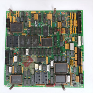
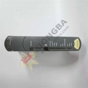
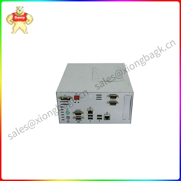
Product Detail: LAM 685-069171-002 Semiconductor Process Chamber Component
Overview
The LAM 685-069171-002 is a precision engineered component designed for use within LAM Research semiconductor processing equipment. This specific part number identifies a critical consumable or replacement item, typically associated with the process chamber of etch or deposition systems. Manufactured to LAM’s exacting specifications, it ensures optimal tool performance, process repeatability, and wafer yield in the production of advanced semiconductor devices.
Key Features & Benefits
• High-Purity Materials: Constructed from materials specifically selected for the semiconductor environment, such as anodized aluminum, ceramic, or specialized coatings, to ensure minimal particle generation and resistance to aggressive process gases (e.g., plasmas).
• Precision Manufacturing: Fabricated to extremely tight tolerances to guarantee perfect fit, form, and function within the designated chamber module, maintaining the original equipment manufacturer’s (OEM) performance standards.
• Process Consistency: Direct OEM replacement part that ensures consistent etch or deposition rates, uniformities, and critical dimensions, directly protecting the value of the wafer-in-process.
• Extended Service Life: Engineered for durability to maximize mean time between replacements (MTBR), reducing tool downtime and total cost of ownership.
• Vacuum Integrity: Designed to maintain the high vacuum integrity required for semiconductor fabrication processes.
685-151509-001
Technical Specifications
Parameter Description
Manufacturer Part Number 685-069171-002
OEM Manufacturer LAM Research Corporation
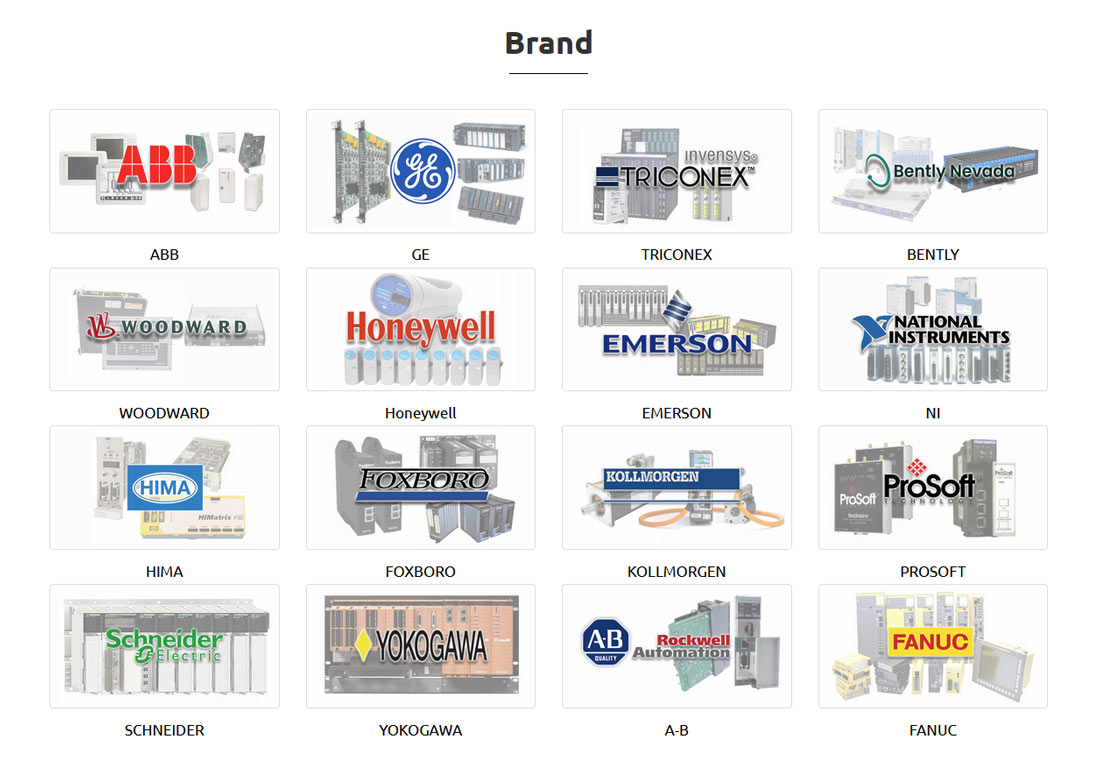
Compatible Tool Families Likely compatible with a range of LAM etch or deposition systems (e.g., 2300® Kiyo®, 2300® Versys®, 2300® Flex® series). Must be verified with compatibility charts.
Component Type Process Chamber Kit, Insulator Ring, Heater, Showerhead, Electrode, Ground Kit, or similar consumable assembly.
Target Application Semiconductor Wafer Fabrication: Dielectric Etch, Silicon Etch, Metal Etch, or Chemical Vapor Deposition (CVD) processes.
Material [e.g., Aluminum Oxide (Al₂O₃) Ceramic, Anodized Aluminum, Quartz, Silicon] Note: Specific material is defined by the part’s function.
Note: The exact specifications, including compatible tool sets and detailed material properties, are defined by LAM Research and must be confirmed using their official documentation.
Typical Applications
This component is a vital spare part used in the maintenance and servicing of LAM Research tools for:
• Plasma Etching: Critical for defining nanoscale features on silicon wafers.
• Chemical Vapor Deposition (CVD): Used in chambers that deposit thin films.
• Chamber Maintenance: Replaced during scheduled preventative maintenance (PM) to restore chamber performance and prevent particle contamination.
• Process Requalification: Essential for bringing a chamber back to specification after service.
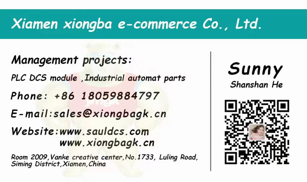
Please contact Sunny sales@xiongbagk.cn for the best price.
➱ sales manager: Sunny
➱ email mailto: sales@xiongbagk.cn
➱ Skype/WeChat: 18059884797
➱ phone/Whatsapp: + 86 18059884797
➱ QQ: 3095989363
➱ Website:www.sauldcs.com