
Description
Product details:
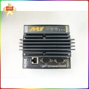
LAM Research 810-495659-313 BICEP ESC POWER SUPPLY
Key words: 810-495659-313
Net weight (Kg) : 2.058Kg
Condition: 100% original
Warranty: 1 year
Packaging: 100% original
Delivery time: TNT, DHL, FEDEX, EMS, UPS
Time of payment: Telegraphic transfer
Delivery time: 3-5 days
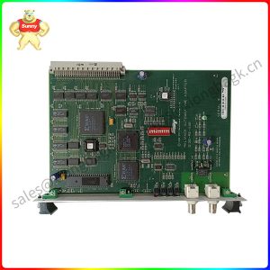
LAM Research 810-495659-303 BICEP ESC Power Supply PCB. Electromagnetic compatibility refers to the ability of electronic devices to work harmoniously and efficiently in various electromagnetic environments. The purpose is to make electronic equipment can not only suppress all kinds of external interference, so that electronic equipment can work normally in the specific electromagnetic environment, but also reduce the electromagnetic interference of electronic equipment itself to other electronic equipment.
1, choose a reasonable wire width because the impact of transient current on the printed line of PCB circuit board is mainly caused by the inductance component of the printed wire, so the inductance of the printed wire should be reduced as far as possible.
2, the use of the correct wiring strategy using equal wiring can reduce the inductance of the wire, but the mutual inductance and distributed capacitance between the wires increase, if the layout allows, it is best to use the zigzag mesh wiring structure, the specific approach is one side of the printed board transverse wiring, the other side longitudinal wiring, and then connected with metallized holes at the cross hole.
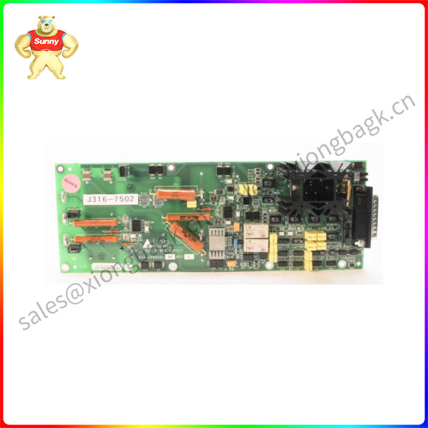
810-495659-303
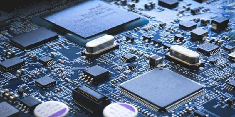
The circuit board includes many types of working layers, such as signal layer, protective layer, screen layer, internal layer, etc. The functions of various layers are briefly described as follows:
⑴ Signal layer: mainly used to place components or wiring. Protel DXP usually contains 30 intermediate layers, namely Mid Layer1~Mid Layer30. The middle layer is used to lay out signal lines, and the top layer and the bottom layer are used to place components or apply copper.
The protective layer: mainly used to ensure that the board does not need tin plating place is not tinned, so as to ensure the reliability of the board operation. Top Paste and Bottom Paste are the top solder resistance layer and the bottom solder resistance layer respectively. Top Solder and Bottom Solder are solder protection layer and bottom solder, respectively.
(3) Screen printing layer: mainly used to print the serial number of components on the circuit board, production number, company name, etc.
| LAM 026182 | 810-069751-114 |
| LAM 600604 | 810-800081-022 |
| LAM 810-800081-005 | 810-072907-005 |
| LAM 716-082039-003 | 810-234640-312 |
| LAM 210024 | 810-001489-016 |
| LAM 3604300 | 810-801237-021 |
| LAM 13-8000-008 | 810-046015-010 |
| LAM 601368 | 810-068158-015 |
| LAM 13-8892-008 | 810-225420-002 |
| LAM 600223 | 810-225420-002 |
Packing and delivery
Whether it is parts, service or delivery efficiency, Moore can do better!!
Xiamen Xiongba supplies 79,928,896 parts to 3,196,226 customers in 151 countries/regions.
➪ condition: new and original packing
➪ warranty: all new parts or repair parts shall have the warranty period of 12 months
➪ payment: inventory goods 100% T/T before shipment
➪ availability: 24/7 service and free online offer
Our mission: to make it easier for customers to buy industrial components
Please contact Sunny sales@xiongbagk.cn for the best price.
➱ sales manager: Sunny
➱ email mailto: sales@xiongbagk.cn
➱ Skype/WeChat: 18059884797
➱ phone/Whatsapp: + 86 18059884797
➱ QQ: 3095989363
➱ Website:www.sauldcs.com