

Description
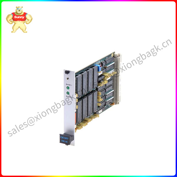
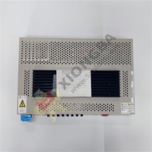
XVME-100 RAMIROM MEMORY MODULE
Thc XVME-100 RAM/ROh? Mcmory Module is a single-high, VMEbus compatible
board, m,hich can accommodate up to 1M byte of RAh‘l, EPROM, or mask
programniablc ROM or 256K bytes of EEPROM. The module is designed with an onboard battery backup circuit to provide power to CMOS RAM devices in the e\cnt
of a power failure.
The XVME-100 has eight 28/32-pin JEDEC sockets which are logically arranged as 2
banks of 4 sockets each. Each bank is designed to employ memory devices oi’ thc
same type and speed, and each bank can be independently configured (T.ia jumpers)
in terms of:
0 VME Address/Memory Chip Size
0 Address Modifier Decode
0 Memory Device Speed
0 Memory Device Pinout
0 Memory Backup Power
The XVME-100 RAAq/ROM Memory Module has power down protection ciriuitr)
\vhich prevents data from being written to memory when the voltage falls below
4.75 Volts. The module also has the option of asserting SYSRESET under this
condition.
XVME-100
This chapter explains how to configure the memory module prior to installation in a
VMEbus system. Included in this chapter is information on jumper options, jumper
locations, and power monitor circuit calibration and installation procedures.
2.2 LOCATION OF COhfPOKENTS KELEVANT TO INSTALLATION
The junipers, memory sockets. and the VMEbus P1 connector on the XVME-100
hkmory Module arc illustrated in Figure 2-1. Figure 2-1A show an expanded left
side of the board, and Figure 2-1B the right for clarification purposes
Thc rollowing five subsections examines thcse juniper options in closer detail,
slio\i7ing spccifically when and how jurnpcrs should be configured.
2.4.1 Jr AI E A (1 dress /hIe in or y C hip Size
12 jumpers exist for each bank (14 total) to dcfinc the VMEbus address and memor)
chip sizc. Table 2-2 lists the jumpers and thcir definitions. The bank \+ill occup!,
a Vl’lEbus address space of four timcs the memory chip sizc. Thc ban!, must bc
assigned to a boundar!, hich is a niultiplc of four timcs the mcmor! chip size.


Please contact Sunny sales@xiongbagk.cn for the best price.
➱ sales manager: Sunny
➱ email mailto: sales@xiongbagk.cn
➱ Skype/WeChat: 18059884797
➱ phone/Whatsapp: + 86 18059884797
➱ QQ: 3095989363
➱ Website:www.sauldcs.com


Reviews
There are no reviews yet.